
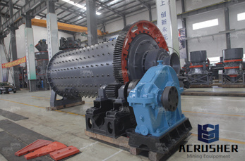
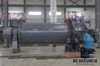
Wafer Back Grinding Process manufacturer Grasping strong production capability, advanced research strength and excellent service, Shanghai Wafer Back Grinding Process supplier create the value and bring values to all of customers.
 WhatsApp)
Semiconductor BackGrinding The silicon wafer on which the active elements are created is a thin circular disc, typically 150mm or 200mm in diameter.
Effect of Wafer Back Grinding on the Mechanical Behavior of Multilayered Lowk for 3DStack Packaging ... generated during wafer back grinding process affect the.
Back grinding is a process that removes silicon from the back surface of a wafer. Silicon Valley Microelectronics provides grinding on our own substrates or on ...
Silicon Wafer Back Grinding Wheel Features Thoroughlymonitored manufacturing process for nearzero scratch Manufactured in clean room class: 100 ~1000
A wafer sawing/grinding process capable of removing cracks and chipping resulted from a wafer sawing operation. A silicon wafer having an active surface and a back ...
Wafer Backgrind is the process of grinding the backside of the wafer to the correct wafer thickness prior to assembly. It is also referred to as ''wafer ...
Figure 1. a) A backgrinding process leaves a characteristic scratch pattern on the back of the wafer. b) The back of the die from certain locations on the wafer have ...
Back Grinding For Bare Device Patterned Wafers,SVM,Inc. Back grinding is a process that removes silicon from the back surface of a ... wafer back grinding process.
BackSide Wafer Grinding Quality Affecting BackEnd Assembly, back grinding process,ABSTRACT Die size and thickness of IC .
GDSI, Grinding and Dicing Services complete resource for Silicon Wafers Processing includes Probing, Bumping, Grinding, Polishing in San Jose, California.
Leadingedge Tape B!_ (B Equipment solution created with semiconductorrelated products ''Adwill.'' Fully and semiautomatic wafer mounters for the dicing process.
Wafer Back Grinding Tapes AI Technology, Inc. Wafer Back Grinding Tapes Rework Process White Papers Wafers requiring grinding and .
UV Tape is adhesive tape for semiconductor process. ... tape holds wafer strongly in wafer grinding process or wafer dicing process. On the other hand, ...
Dec 02, 2014· Grinding a 25Inch F3 Telpe Mirror: Thinning and Flattening the Back Duration: 10:59. GordonWaite 103,343 views. 10:59. Wafer Dicing Process ...
Effects of back grinding process ... Wafer Reclaim and processing services including wafer grinding and thinning, wafer edge trimming, wafer dicing, ...
Offers wafer grinding, dicing, polishing and flip chip service to transfer wafer dice to tape and reel.
Backgrinding. Backgrinding is the process of ... Final outgoing inspection is then carried out before the lot is prepared for shipment back ... Finally, the wafer is ...
Dicing Grinding, Greases, Gels Wax Coatings. Wafer Dicing Tapes; ... Wafer Back Grinding Tapes. ... Consistent bond strength during grinding process;
Introduction of Product Introduction of Wafer Surface Grinding Machine Model GCG300 Junichi Y amazaki Meeting the market requirements for silicon wafers .
Semiconductor Wafer Edge Analysis/4 Stricter requirements in the wafer manufacturing process have made edge measurements important for both 200 mm and 300 mm wafers.
Custom Silicon Wafer Back Grinding Services SVM. Back grinding is a process that removes silicon from the back surface of a wafer Silicon Valley Microelectronics ...
Warping of silicon wafers subjected to backgrinding process. This study investigates warping of silicon wafers in ultraprecision grindingbased backthinning process.
Numerical Simulations of a Back Grinding Process for Silicon. Publication » Numerical Simulations of a Back Grinding Process for Silicon Wafers.
Effect of Wafer Back Grinding on the Mechanical Behavior of Multilayered Lowk for 3DStack Packaging ... generated during wafer back grinding process affect the
WhatsApp)